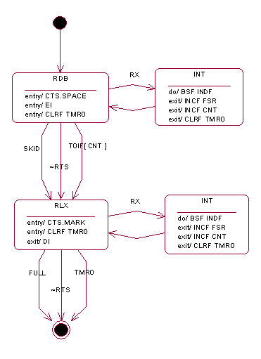
Figure 5 . Receiver State Chart
Application
To test these routines we need a test application. This application should work in two modes: testing the transmitter and testing the receiver. First may be done by sending a sequence of characters 0x20-0xFF to the serial port, latter – by reading data form the port and sending them back. To control the operational mode we may use DTR and RTS lines: SPACE on DTR initiates transmitter test, SPACE on RTS initiates receiver test. All unused memory we may use for RS_BUFFER. To prevent occasional overriding by the receiver routine, when the buffer is overflowed, we may place the buffer after all working registers. If such buffer overflow happens, it may be recognized by presence of zeros in the outgoing stream. Receiver routine implements state chart described above with one derivation – at baud rate 230400 CTS is set MARK in the interrupt routine. At this speed, PIC spends less then 10% of CPU (4 cycles of 47) outside of the interrupt routine, which causes essential delay between detecting that the buffer limit is exceeded and suspending transmission. To avoid this problem the buffer is checked and CTS is set in the interrupt routine. Application source is available in Addendum B.
All aboard
Application schema is given on Figure 6. RS-232-to-TTL converter is implemented on discrete parts V1-V4, D4-D6, R1-R11. Negative voltage is taken from DTR and RTS lines via D5 and D6. V1 and V2 converts TTL to RS-232 levels and drives RX and CTS lines. V3 and V4 converts RS-232 levels to TTL and reads TX and RTS lines. Since input pins RB0, RB6 are pulled down, internal week pull-up should be disabled. R11-D4 serves for reading DTR signal (notice, it is not inverted). Transistors V1-V4 can be any small signal p-n-p with Vce > 25V. I have used KT3107L; BC559C may be used instead. D4 is a small power Zener diode, Ust = 3.7-4.7 V, Ist ~= 10mA.
With this implementation, SPACE is logical ‘0’ and MARK is logical ‘1’. Waveform produced by V1 and V2 is not symmetrical regarding to zero. MARK voltage is about –10V and SPACE is about +5V. Jumpers JP1-JP2 are baud rate selectors (both connected specify 230400). LEDs D1-D2 indicate current state and speed. LED D3 indicates reset and WDT timeout conditions. Pin selection is not critical except the RX pin. Best choice for RX is RB0/INT. If this pin is already in use, a pin with on-change interrupt may also be used. In such case additional care should be taken on ensuring that the interrupt source is RX and that the interrupt flag is cleared after stop bit has started
Post a Comment