This post presents an alternate implementation of SISAM hardware – a “COM2” plug-in. It is designed for plugging in ahead of a bracket DB9 cable, usually used for accommodating a second serial port. This implementation uses a different MCU – PIC16F88, which allows the application to utilize 30% more RAM for the sampling buffer.
Capabilities
SISAM 88 – provides the same set of capabilities as SISAM 690 (differences are underlined/strikethrough):
- S – Sampling single logical channel – RB2
RB5up to 500 ksps (kilo sample per sec) - X – Sampling dual logical channels RB2, RB1
RB5, RB4up to 200 ksps per each channel - J – Limited buffered sampling sole channel @ 5 Msps (2560
1920samples via internal buffer) - M – Measuring pulse timing on RB3
RC5up to 12 kHz average, - o – drive (trigger) four
fiveoutput pins right before (0.8us) sampling starts - O – drive (trigger) four
fiveoutput pins immediately and/or in a sequence (20 us per data byte)
In addition to mentioned above, SISAM can be used as a variable frequency generator (VFG). With the current firmware – as a side effect of S command (a separate command is planned for upcoming firmware updates)
System requirements
- High-speed serial port (such as SerialXP)
- Triple power supply (+5VDC, +12VDC, -12VDC)
Schematics
SISAM88 hardware schematic is given on Figure 1. It includes
- MCU PIC16F88 (U1)
- 20MHz crystal (X1)
- RS232 level converter, build up on SN75150 line driver (U2), current-limiting resistors R1-R3, R6, a Zener diode D1 that prevents RA5/VPP from being pulled up to +12V.
- Current-limiting resistors R4, R5 on input
- Four connectors J1-J4.
J2 is an angled 10 pin male IDC header identical to a COM2 connector on the motherboard. J1 is an angled female IDC header mating with the COM2 connector. J3 is an angled 4 pins header mating with Mini-Molex power connector (FDD power). J4 is a 6 pins header compatible with your ICSP programmer (for example PICkit2).
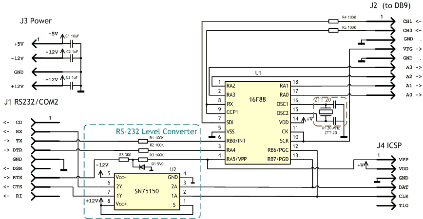
Actuator outputs are connected to RA0-RA3.
Wire RB4-RB5 delivers clock from EUSART to SSP. RB4 also serves as VFG output.
External connectors
Power – it is an altered FDD power connector. 12V ground header is pulled out of it and another header inserted instead. This header is wired to -12VDC.
| Pin # | Description |
|---|---|
| 1 | +5V |
| 2 | -12V |
| 3 | GND |
| 4 | +12V |
Bracket DB9 – it is a standard COM2 bracket cable. In this design it is used as an input/output connector for connecting probes. Pin 5 on this connector is still used for ground to make it compatible with RS232 cables that may have it connected to the chassis. It make safe connecting a regular RS232 cable.
| Pin # | Name | Direction | Description |
|---|---|---|---|
| 1 | CH1 | In | CH1 sampler input |
| 2 | CH0 | In | CH0 sampler input |
| 3 | GND | – | Signal ground |
| 4 | VFG | Out | VFG output |
| 5 | GND | – | Actuator ground |
| 6 | A3 | Out | Actuator line 3 |
| 7 | A2 | Out | Actuator line 2 |
| 8 | A1 | Out | Actuator line 1 |
| 9 | A0 | Out | Actuator line 0 |
Firmware
SISAM v1.1/88 Firmware is available for download.
Revision 1.1 includes the following changes
1. Fixed defect with improper speed estimation for command r02;X0;
Board
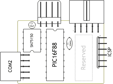
Figure 2 shows the board layout (Scale 1:2). Discrete parts, which are not shown on this layout, are surface mount on the soldering side. PCB layout is not yet ready.
The board has some space reserved for the future upgrades.
ICSP
PIC can be programmed in circuit; however, the device should be disconnected from power supply.
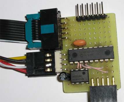
Pictures
 |
 |
 |
 |
| DB9 bracket | SISAM 88 board | Cables connected | SISAM in place |
| Notice altered FDD power connector |
See also: More about SISAM; Simplescope; Overclocking COM port; Downloads
Post a Comment